Introduction to Digital Systems
- System Conversion: Real-world analog signals are captured (e.g., by a microphone) and converted to digital via an ADC (Analog-to-Digital Converter) for processing. After digital processing, a DAC (Digital-to-Analog Converter) translates the signals back to analog for output (e.g., to a speaker).
Binary Logic and Gates
1. Core Concepts
-
Binary Variables: same in discrete mathematics.
-
Logical Operators: same in discrete mathematics. The basic operators are AND, OR, and NOT.
-
Boolean Algebra: same in discrete mathematics.
-
Logic Gates: Physical electronic devices that implement these logic functions.
2. The Basic Logical Operations
-
AND: Denoted by a dot ( \(\cdot\) ) or implied multiplication (e.g., \(X \cdot Y\) or \(XY\)). Output is 1 only if all inputs are 1.
-
OR: Denoted by a plus sign ( \(+\) ) (e.g., \(X + Y\)). Output is 1 if any input is 1.
-
NOT (Inversion): Denoted by an overbar, a single quote, or a tilde (e.g., \(\overline{X}\), \(X'\), or \(\sim X\)). Output is the exact opposite of the input.
3. Truth Tables
- same in discrete mathematics
4. Physical Modeling of Logic Functions (Switch Model)
Logic functions can be intuitively modeled using electrical switches:
-
Inputs: Logic 1 = Switch Closed; Logic 0 = Switch Open.
-
Outputs: Logic 1 = Light On; Logic 0 = Light Off.
-
Logic mapping to circuits:
-
OR Function: Switches connected in parallel. (Closing either switch completes the circuit).
-
AND Function: Switches connected in series. (Both switches must be closed to complete the circuit).
-
NOT Function: Represented by a normally-closed switch. (Applying logic 1 opens the switch, breaking the circuit).
-
-
Note: This switch model is the foundational concept for relay circuits and modern CMOS gate circuits used in digital technology.
5. Logic Gates Overview
Logic gates are categorized by the number of inputs they accept:
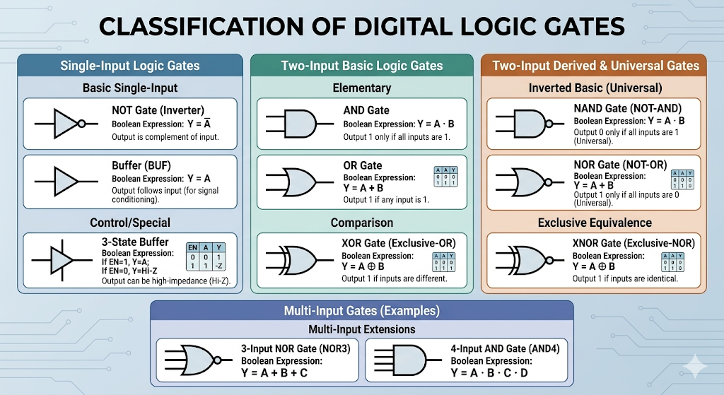
5.1 Single-Input Gates
-
NOT Gate (Inverter): Equation: \(Y = \overline{A}\). Reverses the input.
-
Buffer (BUF): Equation: \(Y = A\). Output matches the input. (Used practically for signal amplification/delay).
5.2 Two-Input Gates
-
AND: Equation: \(Y = AB\)
-
OR: Equation: \(Y = A + B\)
-
XOR (Exclusive-OR): Equation: \(Y = A \oplus B\). Output is 1 if inputs are different (01 or 10).
-
NAND (NOT-AND): Equation: \(Y = \overline{AB}\). The inverse of AND. Output is 0 only when both inputs are 1.
-
NOR (NOT-OR): Equation: \(Y = \overline{A+B}\). The inverse of OR. Output is 1 only when both inputs are 0.
-
XNOR (Exclusive-NOR): Equation: \(Y = \overline{A \oplus B}\). Output is 1 if inputs are the same (00 or 11).
Note: Primitive gates (AND, OR, NOT, NAND, NOR) are simple and fast. Complex circuits use combinations of these to lower cost and transmission time.
5.3 Multiple-Input Gates
Gates can be scaled to accept multiple inputs while following the same underlying logical rules.
-
NOR3: A 3-input NOR gate. Equation: \(Y = \overline{A+B+C}\). Output is 1 only if A, B, and C are all 0.
-
AND4: A 4-input AND gate. Equation: \(Y = ABCD\). Output is 1 only if A, B, C, and D are all 1.
Transistors
1. Evolution of Electronic Switches
-
Relays: Operated mechanically by magnetic fields via energizing coils.
-
Vacuum Tubes: Replaced relays, allowing paths to be opened and closed electronically rather than mechanically.
-
Transistors: The modern standard. They act as miniature electronic switches that control current paths and are the fundamental building blocks of today's digital systems.
2. Silicon and Semiconductors(*)
Transistors are primarily built from silicon.
-
Pure Silicon: Acts as a poor conductor because it lacks free electrical charges.
-
Doped Silicon: Impurities are intentionally added to create free charges, turning it into a good conductor.
-
n-type: Doped to have free negative charges (electrons).
-
p-type: Doped to have free positive charges (holes).
-
3. Integrated Circuits (ICs) and Transistor Families
ICs combine millions of transistors onto a single chip. There are two primary logic families:
-
TTL (Transistor-Transistor Logic): Utilizes Bipolar Junction Transistors (BJTs).
-
CMOS (Complementary Metal-Oxide Semiconductor): Utilizes Field Effect Transistors (FETs). This is the dominant technology today.
-
CMOS Transistors consist of three main terminals: Gate, Source, and Drain.
-
They come in two complementary types: NMOS and PMOS.
-
Integrated Circuit (IC) Parameters
1. Power Supply Voltage (\(V_{CC}\) / \(V_{DD}\))
-
Logic families require a standard operating voltage (e.g., \(5\text{V}\) for older TTL, \(3.3\text{V}\) or lower for modern CMOS).
-
The high voltage is typically denoted as \(V_{CC}\) or \(V_{DD}\), and the ground reference (\(0\text{V}\)) is denoted as \(\text{GND}\) or \(V_{SS}\). These are commonly called "power supply rails."
2. Logic Levels and Noise Margins
Digital systems use discrete voltage ranges rather than exact single voltages to represent \(1\) and \(0\). This makes them robust against noise.
-
Key Voltage Thresholds:
-
\(V_{OH}\): Minimum voltage a gate will output for Logic \(1\) (High).
-
\(V_{OL}\): Maximum voltage a gate will output for Logic \(0\) (Low).
-
\(V_{IH}\): Minimum voltage a gate requires at its input to recognize a Logic \(1\).
-
\(V_{IL}\): Maximum voltage a gate requires at its input to recognize a Logic \(0\).
-
-
Forbidden Zone: The voltage range between \(V_{IL}\) and \(V_{IH}\) where the logic value is undefined/unpredictable.
-
Noise Margins (\(NM\)): The buffer zone that absorbs signal noise without causing logic errors.
- High Noise Margin:
\[ NM_H = V_{OH} - V_{IH} \]-
Low Noise Margin:
\[ NM_L = V_{IL} - V_{OL} \]
3. Timing and Delays
-
Transition Time (Rise/Fall Time): Also known as slew rate. The time it takes for a signal to transition between states, typically measured between the \(10\%\) and \(90\%\) marks of the full voltage swing.
-
\(t_r\): Rise time (Low to High).
-
\(t_f\): Fall time (High to Low).
-
-
Propagation Delay (\(T_{pd}\)): The time delay between an input changing and the corresponding output changing.
-
\(t_{pLH}\): Delay when output switches from Low to High.
-
\(t_{pHL}\): Delay when output switches from High to Low.
-
-
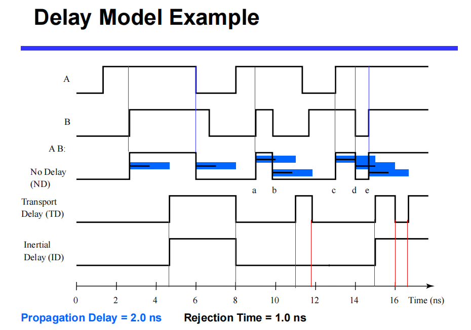
Delay Models:
-
Transport Delay: A fixed, absolute time shift of the signal.
-
Inertial Delay: Accounts for the fact that a circuit requires an input to be held for a minimum duration to register. It rejects very narrow voltage spikes ("pulses") shorter than a specified rejection time.
-
- 图片来自刘海风老师的课件
4. Power Dissipation
The total power a logic gate consumes is the sum of static and dynamic power.
-
Static ("Quiescent") Power (\(P_S\)): Power consumed when the circuit is idle (inputs/outputs are not changing). Caused by leakage current (\(I_{DD}\)). Very low in CMOS devices.
-
\[P_S = I_{DD} \cdot V_{CC}\]
-
-
Dynamic Power (\(P_D\)): Power consumed during switching, primarily due to charging and discharging internal and external capacitances.
-
\[P_D = (C_{PD} + C_L) \cdot V_{CC}^2 \cdot f\]
-
Where \(C_{PD}\) is internal capacitance, \(C_L\) is load capacitance, and \(f\) is the switching frequency.
-
5. Fan-in and Fan-out
-
Fan-in: The maximum number of input signals a single logic gate can accept.
-
Fan-out: The maximum number of standard inputs (loads) that a single gate's output can drive without degrading its normal operation (i.e., without exceeding its maximum specified transition time).
- Note: Fan-out loading directly affects propagation delay. The more gates a driver is connected to, the higher the capacitance, and the slower the delay (e.g., \(t_{pd} = 0.07 + 0.021 \cdot \text{SL ns}\), where \(\text{SL}\) is Standard Loads).
6. Gate Cost
In integrated circuit design, the "cost" of a gate is generally proportional to the chip area it occupies.
-
Area is determined by the number and size of transistors + the amount of wiring connecting them.
-
As a rough, quick metric, gate cost is often approximated by the gate input count. Actual physical layout area remains the most accurate measure.
Boolean Algebra Fundamentals
1. Introduction to Boolean Algebra
- Discrete mathematics
2. Boolean Functions
-
Definition: A Boolean function, \(F = f(X_1, X_2, \dots, X_n)\), is an algebraic expression formed by binary variables (\(X_i\)), constants (\(0\) and \(1\)), logic operation symbols, and parentheses.
-
Once the input signals are fixed, the output signal is fixed.
-
Caution: Standard algebraic rules do not always apply. For example, if \(X + Y = X + Z\), it does not mean \(Y = Z\) in Boolean algebra.
-
-
Representations of Logic Functions:
-
Algebraic Expression: e.g., \(F(X,Y,Z) = X + \overline{Y}Z\). (Note: Expressions are not unique for a given function).
-
Logic Gate Diagram: A physical/schematic drawing using logic gates.
-
Truth Table: Same in discrete mathematics.
-
Waveforms (Timing Diagrams): Graphical representation of inputs and outputs over time.
-
-
Equivalence: Same in discrete mathematics.
3. Operator Precedence
When evaluating a Boolean expression, the order of operations is strictly:
-
Parentheses
() -
NOT
¯or' -
AND
· -
OR
+(Consequence: Parentheses are almost always required around OR expressions if they need to be evaluated before an AND operation, e.g., \(F = A(B + C)\)).
Properties, Identities, and Theorems
1. Basic Identities
-
Including Law (Consensus Theorem): \(AB + \overline{A}C + BC = AB + \overline{A}C \quad | \quad (A+B)(\overline{A}+C)(B+C) = (A+B)(\overline{A}+C)\)
-
Others: see in Discrete mathematics
2. Core Theorems
-
DeMorgan’s Theorem: Inverts an entire expression by breaking the bar and changing the sign.
- Generalized: \(\overline{F(X_1, X_2, \dots, +, \cdot)} = F(\overline{X_1}, \overline{X_2}, \dots, \cdot, +)\)
-
Shannon’s Theorem (Expansion):
- \(F(X_1, X_2, \dots, X_n) = X_1 \cdot F(1, X_2, \dots, X_n) + \overline{X_1} \cdot F(0, X_2, \dots, X_n)\)
3. Complement vs. Duality
-
Complement (\(\overline{F}\)): Represents the exact opposite output of the function. Derived by interchanging \((\cdot \leftrightarrow +)\), interchanging \((1 \leftrightarrow 0)\), AND complementing each variable \((X \leftrightarrow \overline{X})\). (Essentially applying DeMorgan's repeatedly).
-
Dual: Derived by interchanging \((\cdot \leftrightarrow +)\) and interchanging \((1 \leftrightarrow 0)\), but leaving the variables exactly as they are.
- If a Boolean formula is valid, its dual must also be valid. Proving one formula automatically proves its dual.
Canonical and Standard Forms
To systematically design and simplify circuits, functions are expressed in standard formats.
1. Minterms and Maxterms
For a system with \(n\) variables, there are \(2^n\) possible Minterms and Maxterms.
| Feature | Minterm (mi) | Maxterm (Mi) |
|---|---|---|
| Definition | An AND term where every variable is present exactly once (normal or complemented). | An OR term where every variable is present exactly once (normal or complemented). |
| Logic Mapping | Corresponds to exactly one combination in a truth table that produces a 1. | Corresponds to exactly one combination in a truth table that produces a 0. |
| Example (\(X,Y,Z\)) | For inputs 0 0 0, the minterm is \(m_0 = \overline{X}\overline{Y}\overline{Z}\) |
For inputs 0 0 0, the maxterm is \(M_0 = X + Y + Z\) |
| Key Property | Product of any two different Minterms is \(0\) (\(m_i \cdot m_j = 0\)). | Sum of any two different Maxterms is \(1\) (\(M_i + M_j = 1\)). |
| Sum/Product Rule | Sum of all possible Minterms is \(1\) (\(\Sigma m_i = 1\)). | Product of all possible Maxterms is \(0\) (\(\Pi M_i = 0\)). |
-
Relationship: Minterms and Maxterms with the same index are complements of each other: \(M_i = \overline{m_i}\) and \(m_i = \overline{M_i}\).
-
Function Construction: Any Boolean function \(F\) can be written as the sum of its Minterms (\(F = \Sigma m_i\)) or the product of its Maxterms (\(F = \Pi M_i\)).
2. Standard Forms
Standard forms are practical simplifications of canonical forms (they don't require every variable to be in every term).
-
Sum-of-Products (SOP)(DNF in discrete math): Equations written as an OR of AND terms.
-
Example: \(F = AB\overline{C} + BC + B\)
-
Implementation: Naturally maps to a two-level AND-OR gate circuit.
-
-
Product-of-Sums (POS)(CNF in discrete math): Equations written as an AND of OR terms.
-
Example: \(F = (A + B)(\overline{A} + B + \overline{C})C\)
-
Implementation: Naturally maps to a two-level OR-AND gate circuit.
-
3. Simplification Goal
The complexity of a standard form (like Sum-of-Minterms) is often very high. By applying Boolean algebra properties (like the Distributive and Absorptive laws), we can manipulate equations into simpler SOP or POS forms.
Simplification of Logic Functions
1. Measuring Simplicity (Cost Criteria)
Before we can optimize a circuit, we need formal metrics to measure its "cost."
1.1 Literal Cost (\(L\))
-
Definition: The total number of literal appearances in a Boolean expression. (A literal is a variable or its complement, e.g., \(A\) or \(\overline{A}\)).
-
How to count: Simply count every single letter in the equation.
-
Example: \(F = BD + A\overline{B}C + A\overline{C}D\)
-
Calculation: \(2 + 3 + 3 = 8\). Thus, \(L = 8\).
-
1.2 Gate Input Cost (\(G\))
-
Definition: The total number of inputs connected to all the logic gates in the corresponding circuit implementation, excluding inverters (NOT gates).
-
How to count from an SOP/POS equation:
-
Count all literal appearances (\(L\)).
-
Add the number of terms (excluding single-literal terms, because they don't require an AND/OR gate to combine them).
-
Example: \(F = BD + A\overline{B}C + A\overline{C}D\)
-
Calculation: \(L = 8\). There are 3 terms (all multi-literal), requiring a 3-input OR gate. \(G = 8 + 3 = 11\).
-
1.3 Gate Input Cost with NOTs (\(GN\))
-
Definition: The Gate Input Cost (\(G\)), plus the number of inputs to the inverters.
-
How to count: Take \(G\), and add \(1\) for each distinct complemented variable in the equation.
-
Example: \(F = BD + A\overline{B}C + A\overline{C}D\).
-
Calculation: \(G = 11\). We have \(\overline{B}\) and \(\overline{C}\) (2 distinct inverters needed). \(GN = 11 + 2 = 13\)
-
2. Karnaugh Maps (K-Maps)
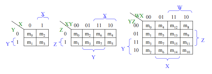
While Boolean algebra is useful, it is often a trial-and-error process. Karnaugh Maps provide a systematic, graphical method for optimizing logic functions (usually up to 4 or 5 variables).
- 图片来自刘海风老师的授课课件
2.1 K-Map Structure and Principles
-
Grid Layout: A 2D matrix with \(2^n\) cells for an \(n\)-variable function. Each cell represents one specific minterm (a row in the truth table).
-
Gray Code Adjacency: The axes are labeled using Gray Code (e.g., \(00, 01, 11, 10\)). This ensures that any two physically adjacent cells differ by exactly one variable.
-
The Core Principle: Because \(AB + A\overline{B} = A\), grouping adjacent cells containing '1's eliminates the variable that changes state between them.
2.2 Definitions
-
Implicant: Any product term that can be formed by grouping valid adjacent '1's.
-
Prime Implicant (PI): An implicant corresponding to the largest possible circle in a K-map. (You cannot absorb it into a larger valid group).
-
Essential Prime Implicant (EPI): A Prime Implicant that covers at least one '1' (minterm) that is not covered by any other Prime Implicant.
2.3 Rules for Grouping (Drawing Circles)
To find the minimum Sum-of-Products (SOP):
-
Size: Circles must cover a number of squares that is a power of 2 (\(1, 2, 4, 8, 16\dots\)).
-
Maximization: Make circles as large as mathematically possible (to eliminate the most variables).
-
Coverage: Every '1' in the map must be circled at least once.
-
Wrapping: The map wraps around! The top edge is adjacent to the bottom edge, and the left edge is adjacent to the right edge.
-
Selection Rule: Start by circling the Essential Prime Implicants (EPIs). Then, select the minimum number of remaining Prime Implicants needed to cover all the leftover '1's.
- Note: Final simplified expressions may not always be unique. There can be multiple equally valid, minimal cost solutions.
2.4 Don't Cares (\(X\))
-
"Don't Cares" are input conditions that will never happen, or outputs we simply don't care about.
-
Rule: You can circle an \(X\) (treat it as a \(1\)) if and only if it helps you make a circle larger. Otherwise, leave it uncircled (treat it as a \(0\)). Never circle a group composed entirely of \(X\)s.
2.5 Examples
Example 1: Basic Grouping (Pairs and Quads)
This example demonstrates how to form basic groups of 2 (pairs) and 4 (quads) in a 3-variable map.
Function: \(F(A, B, C) = \Sigma m(0, 1, 2, 3, 6)\)
Mapping & Grouping:
-
Plot the 1s: Place a
1in cells \(m_0, m_1, m_2, m_3\), and \(m_6\). -
Find the largest groups:
-
Group 1 (Quad): Cells \(m_0, m_1, m_3, m_2\) form a row of four. Looking at the variables, \(A\) is strictly \(0\), while \(B\) and \(C\) change across all possible combinations. The changing variables drop out, leaving \(\overline{A}\).
-
Group 2 (Pair): Cell \(m_6\) is left. It can be grouped with \(m_2\) (vertical pair). For this column, \(B=1\) and \(C=0\), while \(A\) changes from \(0\) to \(1\). Variable \(A\) drops out, leaving \(B\overline{C}\).
-
Simplified SOP Expression:
Example 2: The "Wrap-Around" Adjacency (Edges and Corners)
K-maps are not flat; they wrap around horizontally and vertically. This example shows how to group the four corners.
Function: \(F(A, B, C, D) = \Sigma m(0, 2, 8, 10, 13, 15)\)
Mapping & Grouping:
-
Plot the 1s: Place a
1in the four corners (\(m_0, m_2, m_8, m_{10}\)) and the middle-right (\(m_{13}, m_{15}\)). -
Find the largest groups:
-
Group 1 (Corner Quad): The four corners are logically adjacent. In all four corners, \(B\) is \(0\) and \(D\) is \(0\) (\(A\) and \(C\) change). This extracts the term \(\overline{B}\overline{D}\).
-
Group 2 (Pair): Cells \(m_{13}\) and \(m_{15}\) form a horizontal pair. Here, \(A=1\), \(B=1\), and \(D=1\), while \(C\) changes. This extracts the term \(ABD\).
-
Simplified SOP Expression:
Example 3: Utilizing "Don't Cares" (\(X\))
"Don't Care" conditions (\(X\)) can be treated as either 0 or 1. The rule is: only include an \(X\) if it helps make a group of 1s larger.
Function: \(F(A, B, C, D) = \Sigma m(1, 3, 7, 11, 15) + d(0, 2, 5)\)
(Note: \(\Sigma m\) are the required 1s, \(d\) are the Don't Cares).
Mapping & Grouping:
-
Plot the 1s and Xs: Place
1s in \(m_1, m_3, m_7, m_{11}, m_{15}\). PlaceXs in \(m_0, m_2, m_5\). -
Find the largest groups:
-
Group 1 (Quad): The
1s at \(m_3, m_7, m_{11}, m_{15}\) form a vertical column. Here, \(C=1\) and \(D=1\). Term: \(CD\). -
Group 2 (Quad): We have a
1left at \(m_1\). By treating theXs at \(m_0\) and \(m_2\) as1s, we can combine them with \(m_1\) and \(m_3\) to form a horizontal row of four. Here, \(A=0\) and \(B=0\). Term: \(\overline{A}\overline{B}\). -
Note: We leave the
Xat \(m_5\) as a0because circling it wouldn't help cover any remaining1s.
-
Simplified SOP Expression:
Example 4: Avoiding Redundant Groups (Non-Essential Prime Implicants)
A common mistake is drawing too many circles. You only need the Essential Prime Implicants (EPIs) to cover all the 1s.
Function: \(F(A, B, C, D) = \Sigma m(5, 7, 13, 15, 8, 9, 10, 11)\)
Mapping & Grouping:
-
Plot the 1s: Place
1s in the designated cells. -
Find the groups:
-
Group 1 (Quad - EPI): Cells \(m_5, m_7, m_{13}, m_{15}\) form a square. Term: \(BD\). (This is an EPI because \(m_5\) and \(m_7\) can only be grouped here).
-
Group 2 (Quad - EPI): Cells \(m_8, m_9, m_{10}, m_{11}\) form a horizontal row. Term: \(A\overline{B}\). (This is an EPI because \(m_8\) and \(m_{10}\) can only be grouped here).
-
Group 3 (Redundant Quad): You could draw a square covering \(m_9, m_{11}, m_{13}, m_{15}\) (Term: \(AD\)). However, all of these
1s are already covered by Group 1 and Group 2. This group is a Prime Implicant, but it is not essential. Including it would waste logic gates.
-
Simplified SOP Expression:
3. Advanced Optimization Techniques
3.1 Bubble Pushing
This is a graphical technique based on DeMorgan's Theorem (\(\overline{A \cdot B} = \overline{A} + \overline{B}\) and \(\overline{A+B} = \overline{A} \cdot \overline{B}\)). It is used to determine the Boolean expression of complex circuits built with NAND/NOR gates, or to convert circuits into NAND/NOR logic.
-
Pushing Backward: Move a bubble from the output to the inputs. Change the gate shape (AND \(\leftrightarrow\) OR), and add bubbles to all inputs.
-
Pushing Forward: Move bubbles from all inputs to the output. Change the gate shape (AND \(\leftrightarrow\) OR), and add a bubble to the output.
-
Goal: Draw gates in alternate DeMorgan forms so that bubbles connected by wires "cancel" each other out (an inversion of an inversion is a straight wire).
3.2 Multiple-Level Optimization
Standard K-Maps yield optimal two-level circuits (SOP or POS, which is an AND-layer followed by an OR-layer). However, we can often reduce the gate cost further by factoring the equation into multiple levels.
-
Example Transformation:
-
Start: \(G = ABC + ABD + E + ACF + ADF\) (Cost: 17)
-
Factor \(AB\) and \(AF\): \(G = AB(C+D) + E + AF(C+D)\) (Cost: 13)
-
Factor \((C+D)\): \(G = (AB + AF)(C+D) + E\) (Cost: 12)
-
Factor \(A\): \(G = A(B+F)(C+D) + E\) (Cost: 9)
-
-
By factoring out common terms, we significantly reduced the gate input cost, although we increased the propagation delay by adding more physical layers to the circuit.
Additional Gates and Circuits
1. Exclusive OR (XOR) and Exclusive NOR (XNOR)
1.1 XOR Identities and Properties
Boolean algebra rules apply uniquely to the XOR operator:
-
Identity / Inverse:
-
\(X \oplus 0 = X\)
-
\(X \oplus 1 = \overline{X}\) (Acts as a programmable inverter)
-
\(X \oplus X = 0\)
-
\(X \oplus \overline{X} = 1\)
-
-
Commutative and Associative:
-
\(X \oplus Y = Y \oplus X\)
-
\((X \oplus Y) \oplus Z = X \oplus (Y \oplus Z)\)
-
-
Multiple Variables (Odd vs. Even Functions):
-
Odd Function (XOR): For 3 or more variables (e.g., \(X \oplus Y \oplus Z\)), the output is
1if an odd number of inputs are1. -
Even Function (XNOR): The complement of the odd function. The output is
1if an even number of inputs are1(or if all are zero, depending on the variable count parity).
-
1.2 Implementations and Applications
-
Gate-Level Implementation: XOR is not always a fundamental physical gate; it is often constructed using interconnected standard gates.
-
Major Applications: Extensive use in arithmetic logic circuits (Adders, Subtractors, Multipliers), Counters, and Parity Generators/Checkers.
2. Parity Generators and Checkers
Parity is a simple error-detection mechanism used in data transmission.
-
Parity Bit: An extra bit added to an \(n\)-bit code to produce an \((n+1)\)-bit code word.
-
Even Parity: The parity bit is set so that the total number of
1s in the transmitted message (including the parity bit) is an even number. -
Odd Parity: The parity bit is set so that the total number of
1s is an odd number. -
How it works (Even Parity Example):
-
Generator: Takes the data payload (e.g., \(X,Y,Z\)) and feeds it through an XOR cascade: \(P = X \oplus Y \oplus Z\). If the input has an odd number of
1s, \(P\) becomes1to make the total count even. -
Checker: At the receiving end, the data and the parity bit are checked: \(E = X \oplus Y \oplus Z \oplus P\). If \(E = 0\), the data is accepted (OK). If one bit flipped during transmission causing \(E = 1\), an error is flagged.
-
3. High-Impedance (Hi-Z) and 3-State Buffers
3.1 The "Cannot Do It!" Rule of Standard Gates
Standard logic gates (AND, OR, NOT) always drive their outputs to a 1 (High Voltage) or a 0 (Low Voltage). We cannot physically connect the outputs of standard gates together. If one tries to output 1 (\(V_{CC}\)) and the other outputs 0 (GND), it creates a direct short circuit, destroying the chip.
3.2 The High-Impedance (Hi-Z) State
To solve this, a third electrical state was introduced:
-
1— High voltage -
0— Low voltage -
Hi-Z — High Impedance. It means the output is an open circuit (physically disconnected). It's as if an internal switch has been flipped open, preventing any current from flowing in or out.
3.3 The 3-State Buffer
A special logic gate that provides the Hi-Z state. It has one data input (IN), one data output (OUT), and one control input (EN - Enable).
-
When EN = 1: The buffer is active. OUT = IN (It passes the
1or0through). -
When EN = 0: The buffer is disabled. OUT = Hi-Z. The gate completely disconnects itself from the output wire.
-
Variations: The enable pin (EN) or the input/output pins can be active-low (indicated by a bubble on the symbol).
3.4 Application: Multiplexed Lines
Because 3-state buffers can disconnect themselves, we CAN tie their outputs together onto a single shared wire (a bus), provided we design our control logic so that only one buffer is Enabled (EN=1) at a time. All other buffers must be in the Hi-Z state.
4. Transmission Gates (TG)
-
Concept: A transmission gate is a specific transistor-level design acting as a bidirectional electronic switch. It can connect or disconnect two points in a circuit.
-
Operation:
-
It has an input \(X\), an output \(Y\), and a control signal \(C\).
-
If \(C = 1\), the switch is closed. A direct path exists between \(X\) and \(Y\) (signals can pass).
-
If \(C = 0\), the switch is open. No path exists (equivalent to Hi-Z).
-
-
Usage: They are frequently used inside CMOS ICs to build highly efficient logic circuits, such as building an XOR gate with fewer transistors than standard NAND/NOR logic.